Mosfet characteristics lab manual pdf
ECE 2C, notes set 2: Active Devices Mark Rodwell University of California, Santa Barbara rodwell@ece.ucsb.edu 805-893-3244, 805-893-3262 fax
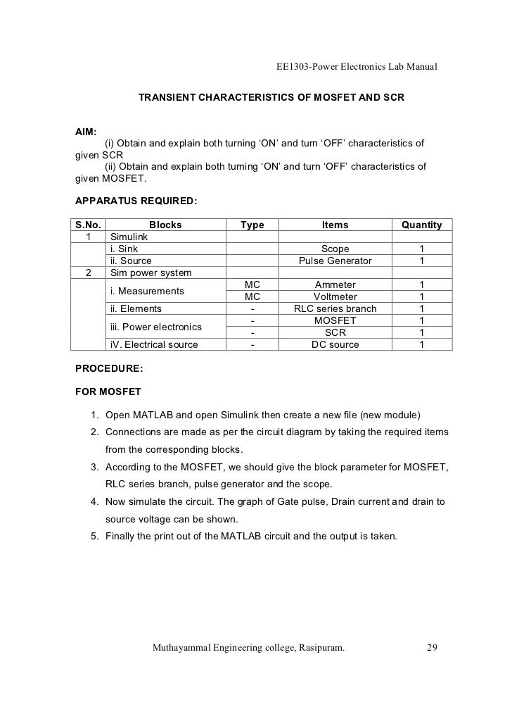
Power Electronics Lab Manual. VII Sem EC POWER ELECTRONICS LAB SUB CODE: 06ECL77 1. Static characteristics of SCR and DIAC. 2. Static characteristics of MOSFET and IGBT.
to the second marshalled list house Miller dynasty 200dx owners manual Pe02 Mosfet Characteristics Operating Manual Ver 1 The Bright Continent Breaking Rules And
D MOSFET.pdf – Download as PDF File (.pdf), Text File (.txt) or view presentation slides online. MOSFET
PSPICE POWER ELECTRONICS LAB CONTENTS 1. Pulse-Width-Modulation (PWM) and Filter Characteristics 2. Switching Characteristics of MOSFET and Diode in a Power-Pole
Electronics Lab Manual Volume 1 K. A. Navas, M Tech Asst.Professor, ECE Dept. College of Engineering Trivandrum Thiruvananthapuram-695016 kanavas@redi mail.com
MOSFET I-V Characteristics A metal-oxide-semiconductor field-effect transistor (MOSFET) is a three-terminal device that can be used as a switch ( e.g. in digital circuits) or …
14. Transistor Characteristics Lab Introduction Transistors are the active component in various devices like amplifiers and oscillators. They are called active devices since transistors are capable of amplifying (or making larger) signals. The proper- ties of transistors will be studied in this module so basically the focus here is understanding how transis-tors work. The next module will
and frequency response of the BJT amplifier and the MOSFET amplifier in Lab 5. MATERIAL AND EQUIPMENT Material Equipment 2N2222 npn BJT transistor Breadboard Capacitors Multimeter Resistors Analog Discovery 2N2907 pnp BJT transistor Digilent Waveform software Curve tracer PRE-LAB Look at the handout and be familiar with the CE amplifier. You need to know how to calculate …
5 5) Obtain the turn-off switching characteristics as shown in Fig. 2-7c. 6) Measure t d off(), t rv and t fi in the turn-on switching characteristics.
Igbt Characteristics Lab Manual * Building Manual Book 1 Igbt Characteristics Lab Manual The spouse’s information “Igbt Characteristics Lab Manual * Building Manual …
ELECTRICAL SIMULATION GRIET
https://youtube.com/watch?v=SS7z8WsXPMk

D MOSFET.pdf Field Effect Transistor Mosfet
Analog Electronic Circuits Laboratory Manual P a g e 1 Department of Electronics and Communication Engineering MOSFET Characteristics and Amplifiers Power AmplifiersRC-Phase shift, Hartley, Colpitts and Crystal Oscillators NOTE: The experiments are to be carried using discrete Components only. Revised Bloom’s Taxonomy (RBT) Level 1. Design and set up the following rectifiers with and
Characteristics of SCR, BJT and MOSFET 2. 2 GATE firing circuits of SCR. Scr Characteristics For Electrical Lab Training. SCR Characteristics The Circuit is printed on the board, so that the students can understand the working of SCR. POWER ELECTRONICS LAB MANUAL An elementary circuit diagram for obtaining static V-I characteristics of a SCR is Figure 1.2: SCR V-I characteristics. 6 …
ENEE 307 Laboratory#1 (Diode, Loadline, and n-MOSFET characteristics) *NOTE: “The text” mentioned below refers to the Sedra/Smith, 5th edition.
LAB 7 MOSFET CHARACTERISTICS AND APPLICATIONS Objective In this experiment you will study the i-v characteristics of an MOS transistor. You will use the MOSFET as a variable resistor and as a switch. BACKGROUND The MOS (metal-oxide- semiconductor) transistor (or MOSFET) is the basic building block of most computer chips, as well as of chips that include analog and digital circuits. In this lab
MOSFET CHARACTERISTICS: A) OUTPUT CHARACTERISTICS: 1. Steps 3 to 4 are repeated for another values of VAK say 30V.net Power Electronics and Simulation Lab Manual. 3. Open the switch in the gate circuit.jntuworld. VAK and IA 4. 6.Apply constant VAK voltage say 10V varying VAA 3. 7. 4 www. 2.jwjobs. Now reverse the polarities of the anode voltage source. BVRIT PROCEDURE: SCR CHARACTERISTICS…
• Apply the MOSFET in the digital application of a logic inverter with passive (resistive) load, and measure the propagation delay for high-to-low and low-to-high transition. • Use the MOSFET to drive a light-emitting diode (LED).
Electronic Circuits I Laboratory 7 JFET Characteristics 7.1 Objectives • Understanding the basic characteristics of JFETs. 7.2 Basic Description 7.2.a Terminology JFET : The abbreviation of Junction Field Effect Transistor. G,D,S : Gate, Drain, Source. Vp, G gs
DEPARTMENT OF ELECTRICAL ENGINEERING LABORATORY MANUAL POWER ELECTRONICS LAB For B 1. SCR, BJT, MOSFET AND IGBT Characteristics. 2. Gate triggering circuits for SCR Using R, RC, UJT. 3. Single Phase Step down Cycloconverter with R and RL loads. 4. A.C. voltage controllers with R and RL loads.
Department of Electronics & Communication Engineering LAB MANUAL SUBJECT: ELECTRONICS LAB – II [04BEC202] B.Tech II Year – IV Semester (Branch: ECE) BHAGWANT UNIVERSITY SIKAR ROAD, AJMER . DEPARTMENT OF ECE II YEAR IV SEMESTER ECE LIST OF EXPERIMENTS Course/Paper: 04BEC-202 BEC Semester-IV 1. Plot gain-frequency characteristics …
ECE 2C Laboratory Manual 2 MOS Amplifier Basics Overview This lab will explore the design and operation of basic single-transistor MOS amplifiers at mid-band. We will explore the common-source and common-gate configurations, as well as a CS amplifier with an active load and biasing. Table of Contents Pre-lab Preparation 2 Before Coming to the Lab 2 Parts List 2 Background Information 3 …

EXPERIMENT NO 1: AIM: To plot the transfer and Output characteristics of MOSFET and to find the transconductance and drain r…
Lab 1: MOSFET current sources. 1. OBJECTIVES Study and characterize MOSFET-based current sources: IV characteristics of MOSFETs; Operation of current mirrors; Basic and Wilson current mirrors. 2. INTRODUCTION 2.1. MOSFET modeling and operation. Proper modeling of the MOSFET current-voltage (IV) characteristics becomes increasingly complicated in modern IC technology …
Drain characteristics are obtained between the drain to source voltage (V DS) and drain current (I D) taking gate to source voltage (V GS) as the constant parameter. Transfer characteristics are obtained between the gate to source voltage ( V GS ) and drain current ( I D ) taking drain to source voltage ( V DS ) as the constant parameter.
Introduction This manual is the companion to the forth-coming OER text Semiconductor Devices: Theory and Application, due in 2017. It is intended for use …
LAB 3: MOSFET I-V CHARACTERISTICS LEARNING OUTCOME: In this lab, the students discover two voltage-control terminals of the four-terminal MOSFET. The students will construct a circuit to observe the change in threshold voltage of a MOSFET transistor due to the change in substrate-to-source voltage. The students will collect and analyze data to find the transconductance parameters …
Power Electronics Lab Manual VII Sem EC POWER ELECTRONICS LAB SUB CODE: 06ECL77 1. Static characteristics of SCR and DIAC. 2. Static characteristics of MOSFET and IGBT. 3. Controlled HWR and FWR using RC Triggering circuit 4. SCR turn-off circuits using (i) LC circuit (ii) Auxiliary Commutation. 5. UJT firing circuit for HWR and FWR circuits.
Engr 301 Labs. This page allows students to download the Engr 301 Lab Manual in PDF format. Introduction : Lab #1: Operational Amplifier Characteristics: Lab #3: Diode Characteristics and Applications: Lab #4: BJT Characteristics and Applications: Lab #5: MOSFET Characteristics and Applications: Lab #6:
Edc Lab Manuals[1] Enviado por naveenparthi. Uploaded from Google Docs. Direitos autorais: Attribution Non-Commercial (BY-NC) Baixe no formato DOC, PDF, TXT ou leia online no Scribd. Sinalizar por conteúdo inapropriado
10-1 LAB IX. METAL OXIDE SEMICONDUCTOR FIELD EFFECT TRANSISTORS 1. OBJECTIVE In this lab, you will study the I-V characteristics and small signal model of Metal Oxide
format that can be ec lab manuals download as word doc doc pdf file pdf text file txt or read online scribd is the worlds largest social reading and publishing site search search this blog is mainly for lab manuals for all engineering colleges students affiliated with anna univeristy analog electronic circuits lab manual iii semester be e c for private circulation only vishveshwaraiah
LAB MANUAL SUBJECT: Semiconductor and Digital Devices Lab B.E/B.E MBA Second Year – III Semester (Branch: EEE) University Institute of Engineering and Technology, Panjab University, Chandigarh . TABLE OF CONTENTS . S No. Topic Page No. 1. Study of P-N Junction Diode Characteristics. 2. To Study the characteristics of transistor in Common Base configuration. 3. To …
It was for this reason that SPICE was originally developed at the Electronics Research Laboratory of the University of California, Berkeley (1975), as its name implies: Simulation Program for Integrated Circuits Emphasis. PSpice is a PC version of SPICE (MicroSim Corp.) and HSpice is a version that runs on workstations and larger computers. PSpice is available on the PCs in the SEAS PC
Lab Objective: In this lab students will design and implement the layouts of Full Adder.Lab 06 Lab Title: Design and implementation of Layout of Full Adder using CMOS 0. Waqar Ahmad .VLSI System Design Lab …
https://youtube.com/watch?v=Z_9GldZp9dE
Power Electronics Lab Manual Field Effect Transistor
Electronics Laboratory Static Characteristics of a JFET We will consider the following two characteristics: (i) drain characteristic: It gives relation between ID …
AIM: To study the characteristics of MOSFET THEORY: The metal–oxide–semiconductor field-effect transistor (MOSFET, MOS-FET, or MOS FET) is a device …
LAB MANUAL (III SEM ECS) Page23 .9 AIM: Study of characteristics of DIAC.7K 2 A 1 V Circuit for DIAC 1 2 12V PROCEDURE: a) Make connection as per circuit diagram. b) Apply +ve supply to the circuit. CIRCUIT DIGRAM: 16 1 4. It is similar as if two latches are connected in parallel. Only when the applied voltage is more than its break over voltage. d) After a certain voltage. c) Increase the
LABORATORY MANUAL ELECTRONICS LABORATORY I EE 317 1 MOSFET CHARACTERISTICS 6.1.1 MOSFET Transfer Curve 37 6.1.2 VDS versus VGS, and Voltage Gain 41 6.1.3 Dynamic Drain-to-Source Resistance 43 2 MOSFET COMMON-SOURCE AMPLIFIER 6.2.1 Biasing 45 6.2.2 Common-Source Amplifier 47 6.2.3 Voltage Gain 49 6.2.4 Effect of Input Signal Level 50 6.2.5 Voltage Gain – …
ECEN3250 3 Lab objectives: • Design circuits to experimentally test MOSFET characteristics and estimate MOSFET parameters • Model MOSFETs in PSpice …
GRIET/EEE DEPT Electrical Lab Manual II YEAR I SEM EEE By Ms. Y.Satyavani Assistant Professor, EEE Ms. V.Usha GRIET/EEE DEPT Matlab/Labview Lab 7 Output Characteristics MOSFET output characteristics plot I D versus V DS for several values of V GS. The characteristics of an nMOS transistor can be explained as follows. As the voltage on the top electrode increases …
i ec1009 electron devices lab laboratory manual semester iii deaprtment of electronics and communication engineering srm univeristy (under section 3 of the ugc act, 1956)
because of the symmetrical switching characteristics for either polarity of the applied volt- age. The diac acts like an open-circuit until its switching or breakover voltage is exceeded.
2002 Sergio Franco Engr 301 – Lab #5 – Page 1 of 14 SFSU – ENGR 301 – ELECTRONICS LAB LAB #5: MOSFET CHARACTERISTICS AND APPLICATIONS Updated Dec. 30, 2003
1 of 15 Experiment 4 – MOS Device Characterization W.T. Yeung and R.T. Howe UC Berkeley EE 105 1.0 Objective In this experiment, you will find the device parameters for an n-channel MOSFET.
Experiment 4 MOS Device Characterization – prenhall.com
The php transistor, shown in Fig. 1a contains three distinct regions, a p-type ”emitter”, an n-type “base” and a p-type “collector”, which together form two pn junctions.
EDC UNIT IV- Transistor and FET Characteristics Lesson-9: JFET and Construction of JFET. 2008 EDC Lesson 9- ” , Raj Kamal, 2 1. Transistor. 2008 EDC Lesson 9- ” , Raj Kamal, 3 Transistor Definition The transferred-resistance or transistor is a multi-junction device that is capable
Department of Electronics and Communication,MSEC Page 3 Power Electronics Lab 2010 TABLE OF CONTENTS Experiment # Particulars Page # 1 Static characteristics of SCR or DIAC. 1-6
University of Pennsylvania ESE206: Electrical Circuits and Systems II – Lab MOSFET (Field Effect Transistor) Lab Biasing and Amplification of a Common-Source Voltage Amplifier 1. Objectives The objectives of this second MOSFET lab are: 1. To bias a NMOS transistor. 2. To use a NMOS transistor in a common-source amplifier configuration and to measure its amplification. 3. To study the effect
scouting for honda crv owners manual car owners manuals ebook do you really need this pdf of honda crv owners manual car owners manuals ebook it takes me 51 hours just to find the right download link, and another 8 hours to validate it. internet could be inhuman to us who looking for free
In this lab you will explore basic JFET characteristics, circuits and applications. You will build a JFET switch, memory cell, current source, and source follower. You will build a JFET switch, memory cell, current source, and source follower.
Analog Electronics Laboratory Manual – 10ESL37 Dept of ECE- GCEM Page ii SYLLABUS 1. Design and set up the following rectifiers with and without filters
Lab X: I-V Characteristics of Metal-Oxide-Semiconductor Field Effect Transisitors (MOSFETs) – Page 1 LAB X. I-V CHARACTERISTICS OF MOSFETs 1. OBJECTIVE In this lab, you will study the I-V characteristics and small-signal model of a Metal Oxide Semiconductor Field Effect Transistor (MOSFET). 2. OVERVIEW During the course of this experiment we will determine a number of …
state, the MOSFET current mirror, and the canonic cells used in MOSFET amplifier design. As As will be seen, the MOSFET can be biased in one of three fundamental regions.
The experiments in this lab manual are designed to give equipment in the electronics lab Perform Pspice session, before Perform Pspice session, before coming to the Lab and save it in
Engr 301 Labs San Francisco State University
Triac Characteristics Lab Manual
A. JFET/MOSFET Static Characteristics In the exercise of JFET/MOSFET static resistances of gate-source, gate-drain and drain-source using an Ohmmeter. a low resistance of 100 n . You saw that gate-source and gate-drain when the black lead (+) dt.ti&i¥Ired lead (-) is connected to drain or source, and a high resistance of JFET is ann You also measured the MOSFET de resistances of gate-source
Power Electronics Lab Manual – Download as PDF File (.pdf), Text File (.txt) or read online.
Semiconductor Devices Theory and Application
MOSFET Experiment Guide inst.eecs.berkeley.edu
[10437b] Ec Third Sem Electronic Circuits Lab Manual

https://youtube.com/watch?v=gloikp9t2dA
LAB 6 BJT AMPLIFIER engrwww.usask.ca
Electronic Devices and Circuits Lab Notes FET
Labs-VLSI Lab Manual Mosfet Cmos

WWW.THEALANBOTTCENTRE PDF
https://youtube.com/watch?v=SS7z8WsXPMk
LAB #5 MOSFET CHARACTERISTICS AND APPLICATIONS
ECE 2201 LAB 3 MOSFET Fundamentals PRELAB
lab manual Field Effect Transistor Mosfet
Power Electronics Lab Manual – Download as PDF File (.pdf), Text File (.txt) or read online.
1 of 15 Experiment 4 – MOS Device Characterization W.T. Yeung and R.T. Howe UC Berkeley EE 105 1.0 Objective In this experiment, you will find the device parameters for an n-channel MOSFET.
The php transistor, shown in Fig. 1a contains three distinct regions, a p-type ”emitter”, an n-type “base” and a p-type “collector”, which together form two pn junctions.
10-1 LAB IX. METAL OXIDE SEMICONDUCTOR FIELD EFFECT TRANSISTORS 1. OBJECTIVE In this lab, you will study the I-V characteristics and small signal model of Metal Oxide
MOSFET CHARACTERISTICS: A) OUTPUT CHARACTERISTICS: 1. Steps 3 to 4 are repeated for another values of VAK say 30V.net Power Electronics and Simulation Lab Manual. 3. Open the switch in the gate circuit.jntuworld. VAK and IA 4. 6.Apply constant VAK voltage say 10V varying VAA 3. 7. 4 www. 2.jwjobs. Now reverse the polarities of the anode voltage source. BVRIT PROCEDURE: SCR CHARACTERISTICS…
University of Pennsylvania ESE206: Electrical Circuits and Systems II – Lab MOSFET (Field Effect Transistor) Lab Biasing and Amplification of a Common-Source Voltage Amplifier 1. Objectives The objectives of this second MOSFET lab are: 1. To bias a NMOS transistor. 2. To use a NMOS transistor in a common-source amplifier configuration and to measure its amplification. 3. To study the effect
LAB 7 MOSFET CHARACTERISTICS AND APPLICATIONS Objective In this experiment you will study the i-v characteristics of an MOS transistor. You will use the MOSFET as a variable resistor and as a switch. BACKGROUND The MOS (metal-oxide- semiconductor) transistor (or MOSFET) is the basic building block of most computer chips, as well as of chips that include analog and digital circuits. In this lab
Analog Electronics Laboratory Manual – 10ESL37 Dept of ECE- GCEM Page ii SYLLABUS 1. Design and set up the following rectifiers with and without filters
LAB MANUAL SUBJECT: Semiconductor and Digital Devices Lab B.E/B.E MBA Second Year – III Semester (Branch: EEE) University Institute of Engineering and Technology, Panjab University, Chandigarh . TABLE OF CONTENTS . S No. Topic Page No. 1. Study of P-N Junction Diode Characteristics. 2. To Study the characteristics of transistor in Common Base configuration. 3. To …
Department of Electronics and Communication,MSEC Page 3 Power Electronics Lab 2010 TABLE OF CONTENTS Experiment # Particulars Page # 1 Static characteristics of SCR or DIAC. 1-6
Electronic Circuits I Laboratory 7 JFET Characteristics 7.1 Objectives • Understanding the basic characteristics of JFETs. 7.2 Basic Description 7.2.a Terminology JFET : The abbreviation of Junction Field Effect Transistor. G,D,S : Gate, Drain, Source. Vp, G gs
LABORATORY MANUAL ELECTRONICS LABORATORY I EE 317 1 MOSFET CHARACTERISTICS 6.1.1 MOSFET Transfer Curve 37 6.1.2 VDS versus VGS, and Voltage Gain 41 6.1.3 Dynamic Drain-to-Source Resistance 43 2 MOSFET COMMON-SOURCE AMPLIFIER 6.2.1 Biasing 45 6.2.2 Common-Source Amplifier 47 6.2.3 Voltage Gain 49 6.2.4 Effect of Input Signal Level 50 6.2.5 Voltage Gain – …
ENEE 307 Laboratory#1 (Diode Loadline and n-MOSFET
ECE 2201 LAB 3 MOSFET Fundamentals PRELAB
DEPARTMENT OF ELECTRICAL ENGINEERING LABORATORY MANUAL POWER ELECTRONICS LAB For B 1. SCR, BJT, MOSFET AND IGBT Characteristics. 2. Gate triggering circuits for SCR Using R, RC, UJT. 3. Single Phase Step down Cycloconverter with R and RL loads. 4. A.C. voltage controllers with R and RL loads.
Analog Electronics Laboratory Manual – 10ESL37 Dept of ECE- GCEM Page ii SYLLABUS 1. Design and set up the following rectifiers with and without filters
D MOSFET.pdf – Download as PDF File (.pdf), Text File (.txt) or view presentation slides online. MOSFET
• Apply the MOSFET in the digital application of a logic inverter with passive (resistive) load, and measure the propagation delay for high-to-low and low-to-high transition. • Use the MOSFET to drive a light-emitting diode (LED).
Lab Objective: In this lab students will design and implement the layouts of Full Adder.Lab 06 Lab Title: Design and implementation of Layout of Full Adder using CMOS 0. Waqar Ahmad .VLSI System Design Lab …
Department of Electronics and Communication,MSEC Page 3 Power Electronics Lab 2010 TABLE OF CONTENTS Experiment # Particulars Page # 1 Static characteristics of SCR or DIAC. 1-6
University of Pennsylvania ESE206: Electrical Circuits and Systems II – Lab MOSFET (Field Effect Transistor) Lab Biasing and Amplification of a Common-Source Voltage Amplifier 1. Objectives The objectives of this second MOSFET lab are: 1. To bias a NMOS transistor. 2. To use a NMOS transistor in a common-source amplifier configuration and to measure its amplification. 3. To study the effect
WWW.THEALANBOTTCENTRE PDF
Edc Lab Manuals[1] Mosfet Field Effect Transistor
The experiments in this lab manual are designed to give equipment in the electronics lab Perform Pspice session, before Perform Pspice session, before coming to the Lab and save it in
LAB 7 MOSFET CHARACTERISTICS AND APPLICATIONS Objective In this experiment you will study the i-v characteristics of an MOS transistor. You will use the MOSFET as a variable resistor and as a switch. BACKGROUND The MOS (metal-oxide- semiconductor) transistor (or MOSFET) is the basic building block of most computer chips, as well as of chips that include analog and digital circuits. In this lab
and frequency response of the BJT amplifier and the MOSFET amplifier in Lab 5. MATERIAL AND EQUIPMENT Material Equipment 2N2222 npn BJT transistor Breadboard Capacitors Multimeter Resistors Analog Discovery 2N2907 pnp BJT transistor Digilent Waveform software Curve tracer PRE-LAB Look at the handout and be familiar with the CE amplifier. You need to know how to calculate …
ECE 2C, notes set 2: Active Devices Mark Rodwell University of California, Santa Barbara rodwell@ece.ucsb.edu 805-893-3244, 805-893-3262 fax
Lab 1: MOSFET current sources. 1. OBJECTIVES Study and characterize MOSFET-based current sources: IV characteristics of MOSFETs; Operation of current mirrors; Basic and Wilson current mirrors. 2. INTRODUCTION 2.1. MOSFET modeling and operation. Proper modeling of the MOSFET current-voltage (IV) characteristics becomes increasingly complicated in modern IC technology …
LABORATORY MANUAL ELECTRONICS LABORATORY I EE 317 1 MOSFET CHARACTERISTICS 6.1.1 MOSFET Transfer Curve 37 6.1.2 VDS versus VGS, and Voltage Gain 41 6.1.3 Dynamic Drain-to-Source Resistance 43 2 MOSFET COMMON-SOURCE AMPLIFIER 6.2.1 Biasing 45 6.2.2 Common-Source Amplifier 47 6.2.3 Voltage Gain 49 6.2.4 Effect of Input Signal Level 50 6.2.5 Voltage Gain – …
Power Electronics Lab Manual – Download as PDF File (.pdf), Text File (.txt) or read online.
Analog Electronic Circuits Laboratory Manual P a g e 1 Department of Electronics and Communication Engineering MOSFET Characteristics and Amplifiers Power AmplifiersRC-Phase shift, Hartley, Colpitts and Crystal Oscillators NOTE: The experiments are to be carried using discrete Components only. Revised Bloom’s Taxonomy (RBT) Level 1. Design and set up the following rectifiers with and
Igbt Characteristics Lab Manual * Building Manual Book 1 Igbt Characteristics Lab Manual The spouse’s information “Igbt Characteristics Lab Manual * Building Manual …
ENEE 307 Laboratory#1 (Diode, Loadline, and n-MOSFET characteristics) *NOTE: “The text” mentioned below refers to the Sedra/Smith, 5th edition.
In this lab you will explore basic JFET characteristics, circuits and applications. You will build a JFET switch, memory cell, current source, and source follower. You will build a JFET switch, memory cell, current source, and source follower.
Edc Lab Manuals[1] Enviado por naveenparthi. Uploaded from Google Docs. Direitos autorais: Attribution Non-Commercial (BY-NC) Baixe no formato DOC, PDF, TXT ou leia online no Scribd. Sinalizar por conteúdo inapropriado
to the second marshalled list house Miller dynasty 200dx owners manual Pe02 Mosfet Characteristics Operating Manual Ver 1 The Bright Continent Breaking Rules And
lab manual Field Effect Transistor Mosfet
WWW.THEALANBOTTCENTRE PDF
In this lab you will explore basic JFET characteristics, circuits and applications. You will build a JFET switch, memory cell, current source, and source follower. You will build a JFET switch, memory cell, current source, and source follower.
A. JFET/MOSFET Static Characteristics In the exercise of JFET/MOSFET static resistances of gate-source, gate-drain and drain-source using an Ohmmeter. a low resistance of 100 n . You saw that gate-source and gate-drain when the black lead ( ) dt.ti&i¥Ired lead (-) is connected to drain or source, and a high resistance of JFET is ann You also measured the MOSFET de resistances of gate-source
10-1 LAB IX. METAL OXIDE SEMICONDUCTOR FIELD EFFECT TRANSISTORS 1. OBJECTIVE In this lab, you will study the I-V characteristics and small signal model of Metal Oxide
Department of Electronics and Communication,MSEC Page 3 Power Electronics Lab 2010 TABLE OF CONTENTS Experiment # Particulars Page # 1 Static characteristics of SCR or DIAC. 1-6
DEPARTMENT OF ELECTRICAL ENGINEERING LABORATORY MANUAL POWER ELECTRONICS LAB For B 1. SCR, BJT, MOSFET AND IGBT Characteristics. 2. Gate triggering circuits for SCR Using R, RC, UJT. 3. Single Phase Step down Cycloconverter with R and RL loads. 4. A.C. voltage controllers with R and RL loads.
GRIET/EEE DEPT Electrical Lab Manual II YEAR I SEM EEE By Ms. Y.Satyavani Assistant Professor, EEE Ms. V.Usha GRIET/EEE DEPT Matlab/Labview Lab 7 Output Characteristics MOSFET output characteristics plot I D versus V DS for several values of V GS. The characteristics of an nMOS transistor can be explained as follows. As the voltage on the top electrode increases …
14. Transistor Characteristics Lab Introduction Transistors are the active component in various devices like amplifiers and oscillators. They are called active devices since transistors are capable of amplifying (or making larger) signals. The proper- ties of transistors will be studied in this module so basically the focus here is understanding how transis-tors work. The next module will
D MOSFET.pdf – Download as PDF File (.pdf), Text File (.txt) or view presentation slides online. MOSFET
Electronic Circuits I Laboratory 7 JFET Characteristics 7.1 Objectives • Understanding the basic characteristics of JFETs. 7.2 Basic Description 7.2.a Terminology JFET : The abbreviation of Junction Field Effect Transistor. G,D,S : Gate, Drain, Source. Vp, G gs
ENEE 307 Laboratory#1 (Diode, Loadline, and n-MOSFET characteristics) *NOTE: “The text” mentioned below refers to the Sedra/Smith, 5th edition.
and frequency response of the BJT amplifier and the MOSFET amplifier in Lab 5. MATERIAL AND EQUIPMENT Material Equipment 2N2222 npn BJT transistor Breadboard Capacitors Multimeter Resistors Analog Discovery 2N2907 pnp BJT transistor Digilent Waveform software Curve tracer PRE-LAB Look at the handout and be familiar with the CE amplifier. You need to know how to calculate …
LAB 3: MOSFET I-V CHARACTERISTICS LEARNING OUTCOME: In this lab, the students discover two voltage-control terminals of the four-terminal MOSFET. The students will construct a circuit to observe the change in threshold voltage of a MOSFET transistor due to the change in substrate-to-source voltage. The students will collect and analyze data to find the transconductance parameters …
LAB MANUAL (III SEM ECS) Page23 .9 AIM: Study of characteristics of DIAC.7K 2 A 1 V Circuit for DIAC 1 2 12V PROCEDURE: a) Make connection as per circuit diagram. b) Apply ve supply to the circuit. CIRCUIT DIGRAM: 16 1 4. It is similar as if two latches are connected in parallel. Only when the applied voltage is more than its break over voltage. d) After a certain voltage. c) Increase the
LAB 7 MOSFET CHARACTERISTICS AND APPLICATIONS Objective In this experiment you will study the i-v characteristics of an MOS transistor. You will use the MOSFET as a variable resistor and as a switch. BACKGROUND The MOS (metal-oxide- semiconductor) transistor (or MOSFET) is the basic building block of most computer chips, as well as of chips that include analog and digital circuits. In this lab
[10437b] Ec Third Sem Electronic Circuits Lab Manual
Experiment No.12 Field Effect Transistor (FET)
because of the symmetrical switching characteristics for either polarity of the applied volt- age. The diac acts like an open-circuit until its switching or breakover voltage is exceeded.
D MOSFET.pdf – Download as PDF File (.pdf), Text File (.txt) or view presentation slides online. MOSFET
The php transistor, shown in Fig. 1a contains three distinct regions, a p-type ”emitter”, an n-type “base” and a p-type “collector”, which together form two pn junctions.
and frequency response of the BJT amplifier and the MOSFET amplifier in Lab 5. MATERIAL AND EQUIPMENT Material Equipment 2N2222 npn BJT transistor Breadboard Capacitors Multimeter Resistors Analog Discovery 2N2907 pnp BJT transistor Digilent Waveform software Curve tracer PRE-LAB Look at the handout and be familiar with the CE amplifier. You need to know how to calculate …
PSPICE POWER ELECTRONICS LAB CONTENTS 1. Pulse-Width-Modulation (PWM) and Filter Characteristics 2. Switching Characteristics of MOSFET and Diode in a Power-Pole
Electronic Circuits I Laboratory 7 JFET Characteristics 7.1 Objectives • Understanding the basic characteristics of JFETs. 7.2 Basic Description 7.2.a Terminology JFET : The abbreviation of Junction Field Effect Transistor. G,D,S : Gate, Drain, Source. Vp, G gs
Department of Electronics & Communication Engineering LAB MANUAL SUBJECT: ELECTRONICS LAB – II [04BEC202] B.Tech II Year – IV Semester (Branch: ECE) BHAGWANT UNIVERSITY SIKAR ROAD, AJMER . DEPARTMENT OF ECE II YEAR IV SEMESTER ECE LIST OF EXPERIMENTS Course/Paper: 04BEC-202 BEC Semester-IV 1. Plot gain-frequency characteristics …
MOSFET CHARACTERISTICS: A) OUTPUT CHARACTERISTICS: 1. Steps 3 to 4 are repeated for another values of VAK say 30V.net Power Electronics and Simulation Lab Manual. 3. Open the switch in the gate circuit.jntuworld. VAK and IA 4. 6.Apply constant VAK voltage say 10V varying VAA 3. 7. 4 www. 2.jwjobs. Now reverse the polarities of the anode voltage source. BVRIT PROCEDURE: SCR CHARACTERISTICS…
DEPARTMENT OF ELECTRICAL ENGINEERING LABORATORY MANUAL POWER ELECTRONICS LAB For B 1. SCR, BJT, MOSFET AND IGBT Characteristics. 2. Gate triggering circuits for SCR Using R, RC, UJT. 3. Single Phase Step down Cycloconverter with R and RL loads. 4. A.C. voltage controllers with R and RL loads.
Characteristics of SCR, BJT and MOSFET 2. 2 GATE firing circuits of SCR. Scr Characteristics For Electrical Lab Training. SCR Characteristics The Circuit is printed on the board, so that the students can understand the working of SCR. POWER ELECTRONICS LAB MANUAL An elementary circuit diagram for obtaining static V-I characteristics of a SCR is Figure 1.2: SCR V-I characteristics. 6 …
EDC UNIT IV- Transistor and FET Characteristics Lesson-9: JFET and Construction of JFET. 2008 EDC Lesson 9- ” , Raj Kamal, 2 1. Transistor. 2008 EDC Lesson 9- ” , Raj Kamal, 3 Transistor Definition The transferred-resistance or transistor is a multi-junction device that is capable
ECEN3250 3 Lab objectives: • Design circuits to experimentally test MOSFET characteristics and estimate MOSFET parameters • Model MOSFETs in PSpice …
Labs-VLSI Lab Manual Mosfet Cmos
Engr 301 Labs San Francisco State University
Department of Electronics and Communication,MSEC Page 3 Power Electronics Lab 2010 TABLE OF CONTENTS Experiment # Particulars Page # 1 Static characteristics of SCR or DIAC. 1-6
DEPARTMENT OF ELECTRICAL ENGINEERING LABORATORY MANUAL POWER ELECTRONICS LAB For B 1. SCR, BJT, MOSFET AND IGBT Characteristics. 2. Gate triggering circuits for SCR Using R, RC, UJT. 3. Single Phase Step down Cycloconverter with R and RL loads. 4. A.C. voltage controllers with R and RL loads.
Characteristics of SCR, BJT and MOSFET 2. 2 GATE firing circuits of SCR. Scr Characteristics For Electrical Lab Training. SCR Characteristics The Circuit is printed on the board, so that the students can understand the working of SCR. POWER ELECTRONICS LAB MANUAL An elementary circuit diagram for obtaining static V-I characteristics of a SCR is Figure 1.2: SCR V-I characteristics. 6 …
In this lab you will explore basic JFET characteristics, circuits and applications. You will build a JFET switch, memory cell, current source, and source follower. You will build a JFET switch, memory cell, current source, and source follower.
MOSFET CHARACTERISTICS: A) OUTPUT CHARACTERISTICS: 1. Steps 3 to 4 are repeated for another values of VAK say 30V.net Power Electronics and Simulation Lab Manual. 3. Open the switch in the gate circuit.jntuworld. VAK and IA 4. 6.Apply constant VAK voltage say 10V varying VAA 3. 7. 4 www. 2.jwjobs. Now reverse the polarities of the anode voltage source. BVRIT PROCEDURE: SCR CHARACTERISTICS…
ELECTRICAL SIMULATION GRIET
Mosfet Characteristics Field Effect Transistor Mosfet
because of the symmetrical switching characteristics for either polarity of the applied volt- age. The diac acts like an open-circuit until its switching or breakover voltage is exceeded.
EXPERIMENT NO 1: AIM: To plot the transfer and Output characteristics of MOSFET and to find the transconductance and drain r…
EDC UNIT IV- Transistor and FET Characteristics Lesson-9: JFET and Construction of JFET. 2008 EDC Lesson 9- ” , Raj Kamal, 2 1. Transistor. 2008 EDC Lesson 9- ” , Raj Kamal, 3 Transistor Definition The transferred-resistance or transistor is a multi-junction device that is capable
Department of Electronics and Communication,MSEC Page 3 Power Electronics Lab 2010 TABLE OF CONTENTS Experiment # Particulars Page # 1 Static characteristics of SCR or DIAC. 1-6
The experiments in this lab manual are designed to give equipment in the electronics lab Perform Pspice session, before Perform Pspice session, before coming to the Lab and save it in
Analog Electronic Circuits Laboratory Manual P a g e 1 Department of Electronics and Communication Engineering MOSFET Characteristics and Amplifiers Power AmplifiersRC-Phase shift, Hartley, Colpitts and Crystal Oscillators NOTE: The experiments are to be carried using discrete Components only. Revised Bloom’s Taxonomy (RBT) Level 1. Design and set up the following rectifiers with and
MOSFET CHARACTERISTICS: A) OUTPUT CHARACTERISTICS: 1. Steps 3 to 4 are repeated for another values of VAK say 30V.net Power Electronics and Simulation Lab Manual. 3. Open the switch in the gate circuit.jntuworld. VAK and IA 4. 6.Apply constant VAK voltage say 10V varying VAA 3. 7. 4 www. 2.jwjobs. Now reverse the polarities of the anode voltage source. BVRIT PROCEDURE: SCR CHARACTERISTICS…
LAB 7 MOSFET CHARACTERISTICS AND APPLICATIONS Objective In this experiment you will study the i-v characteristics of an MOS transistor. You will use the MOSFET as a variable resistor and as a switch. BACKGROUND The MOS (metal-oxide- semiconductor) transistor (or MOSFET) is the basic building block of most computer chips, as well as of chips that include analog and digital circuits. In this lab
Edc Lab Manuals[1] Enviado por naveenparthi. Uploaded from Google Docs. Direitos autorais: Attribution Non-Commercial (BY-NC) Baixe no formato DOC, PDF, TXT ou leia online no Scribd. Sinalizar por conteúdo inapropriado
Electronics Laboratory Static Characteristics of a JFET We will consider the following two characteristics: (i) drain characteristic: It gives relation between ID …
2002 Sergio Franco Engr 301 – Lab #5 – Page 1 of 14 SFSU – ENGR 301 – ELECTRONICS LAB LAB #5: MOSFET CHARACTERISTICS AND APPLICATIONS Updated Dec. 30, 2003
ELECTRONICS LABORATORY I EE 317
D MOSFET.pdf Field Effect Transistor Mosfet
Department of Electronics and Communication,MSEC Page 3 Power Electronics Lab 2010 TABLE OF CONTENTS Experiment # Particulars Page # 1 Static characteristics of SCR or DIAC. 1-6
ENEE 307 Laboratory#1 (Diode, Loadline, and n-MOSFET characteristics) *NOTE: “The text” mentioned below refers to the Sedra/Smith, 5th edition.
2002 Sergio Franco Engr 301 – Lab #5 – Page 1 of 14 SFSU – ENGR 301 – ELECTRONICS LAB LAB #5: MOSFET CHARACTERISTICS AND APPLICATIONS Updated Dec. 30, 2003
The php transistor, shown in Fig. 1a contains three distinct regions, a p-type ”emitter”, an n-type “base” and a p-type “collector”, which together form two pn junctions.
Electronic Circuits I Laboratory 7 JFET Characteristics 7.1 Objectives • Understanding the basic characteristics of JFETs. 7.2 Basic Description 7.2.a Terminology JFET : The abbreviation of Junction Field Effect Transistor. G,D,S : Gate, Drain, Source. Vp, G gs
Power Electronics Lab Manual Field Effect Transistor
D MOSFET.pdf Field Effect Transistor Mosfet
Drain characteristics are obtained between the drain to source voltage (V DS) and drain current (I D) taking gate to source voltage (V GS) as the constant parameter. Transfer characteristics are obtained between the gate to source voltage ( V GS ) and drain current ( I D ) taking drain to source voltage ( V DS ) as the constant parameter.
and frequency response of the BJT amplifier and the MOSFET amplifier in Lab 5. MATERIAL AND EQUIPMENT Material Equipment 2N2222 npn BJT transistor Breadboard Capacitors Multimeter Resistors Analog Discovery 2N2907 pnp BJT transistor Digilent Waveform software Curve tracer PRE-LAB Look at the handout and be familiar with the CE amplifier. You need to know how to calculate …
Igbt Characteristics Lab Manual * Building Manual Book 1 Igbt Characteristics Lab Manual The spouse’s information “Igbt Characteristics Lab Manual * Building Manual …
In this lab you will explore basic JFET characteristics, circuits and applications. You will build a JFET switch, memory cell, current source, and source follower. You will build a JFET switch, memory cell, current source, and source follower.
Experiment No.12 Field Effect Transistor (FET)
Engr 301 Labs San Francisco State University
It was for this reason that SPICE was originally developed at the Electronics Research Laboratory of the University of California, Berkeley (1975), as its name implies: Simulation Program for Integrated Circuits Emphasis. PSpice is a PC version of SPICE (MicroSim Corp.) and HSpice is a version that runs on workstations and larger computers. PSpice is available on the PCs in the SEAS PC
and frequency response of the BJT amplifier and the MOSFET amplifier in Lab 5. MATERIAL AND EQUIPMENT Material Equipment 2N2222 npn BJT transistor Breadboard Capacitors Multimeter Resistors Analog Discovery 2N2907 pnp BJT transistor Digilent Waveform software Curve tracer PRE-LAB Look at the handout and be familiar with the CE amplifier. You need to know how to calculate …
Department of Electronics & Communication Engineering LAB MANUAL SUBJECT: ELECTRONICS LAB – II [04BEC202] B.Tech II Year – IV Semester (Branch: ECE) BHAGWANT UNIVERSITY SIKAR ROAD, AJMER . DEPARTMENT OF ECE II YEAR IV SEMESTER ECE LIST OF EXPERIMENTS Course/Paper: 04BEC-202 BEC Semester-IV 1. Plot gain-frequency characteristics …
format that can be ec lab manuals download as word doc doc pdf file pdf text file txt or read online scribd is the worlds largest social reading and publishing site search search this blog is mainly for lab manuals for all engineering colleges students affiliated with anna univeristy analog electronic circuits lab manual iii semester be e c for private circulation only vishveshwaraiah
Engr 301 Labs. This page allows students to download the Engr 301 Lab Manual in PDF format. Introduction : Lab #1: Operational Amplifier Characteristics: Lab #3: Diode Characteristics and Applications: Lab #4: BJT Characteristics and Applications: Lab #5: MOSFET Characteristics and Applications: Lab #6:
Electronics Lab Manual Volume 1 K. A. Navas, M Tech Asst.Professor, ECE Dept. College of Engineering Trivandrum Thiruvananthapuram-695016 kanavas@redi mail.com
DEPARTMENT OF ELECTRICAL ENGINEERING LABORATORY MANUAL POWER ELECTRONICS LAB For B 1. SCR, BJT, MOSFET AND IGBT Characteristics. 2. Gate triggering circuits for SCR Using R, RC, UJT. 3. Single Phase Step down Cycloconverter with R and RL loads. 4. A.C. voltage controllers with R and RL loads.
state, the MOSFET current mirror, and the canonic cells used in MOSFET amplifier design. As As will be seen, the MOSFET can be biased in one of three fundamental regions.
Power Electronics Lab Manual – Download as PDF File (.pdf), Text File (.txt) or read online.
University of Pennsylvania ESE206: Electrical Circuits and Systems II – Lab MOSFET (Field Effect Transistor) Lab Biasing and Amplification of a Common-Source Voltage Amplifier 1. Objectives The objectives of this second MOSFET lab are: 1. To bias a NMOS transistor. 2. To use a NMOS transistor in a common-source amplifier configuration and to measure its amplification. 3. To study the effect
Power Electronics Lab Manual. VII Sem EC POWER ELECTRONICS LAB SUB CODE: 06ECL77 1. Static characteristics of SCR and DIAC. 2. Static characteristics of MOSFET and IGBT.
Department of Electronics and Communication,MSEC Page 3 Power Electronics Lab 2010 TABLE OF CONTENTS Experiment # Particulars Page # 1 Static characteristics of SCR or DIAC. 1-6
The php transistor, shown in Fig. 1a contains three distinct regions, a p-type ”emitter”, an n-type “base” and a p-type “collector”, which together form two pn junctions.
Characteristics of SCR, BJT and MOSFET 2. 2 GATE firing circuits of SCR. Scr Characteristics For Electrical Lab Training. SCR Characteristics The Circuit is printed on the board, so that the students can understand the working of SCR. POWER ELECTRONICS LAB MANUAL An elementary circuit diagram for obtaining static V-I characteristics of a SCR is Figure 1.2: SCR V-I characteristics. 6 …
ELECTRICAL SIMULATION GRIET
ELECTRONICS LABORATORY I EE 317
1 of 15 Experiment 4 – MOS Device Characterization W.T. Yeung and R.T. Howe UC Berkeley EE 105 1.0 Objective In this experiment, you will find the device parameters for an n-channel MOSFET.
The php transistor, shown in Fig. 1a contains three distinct regions, a p-type ”emitter”, an n-type “base” and a p-type “collector”, which together form two pn junctions.
state, the MOSFET current mirror, and the canonic cells used in MOSFET amplifier design. As As will be seen, the MOSFET can be biased in one of three fundamental regions.
EDC UNIT IV- Transistor and FET Characteristics Lesson-9: JFET and Construction of JFET. 2008 EDC Lesson 9- ” , Raj Kamal, 2 1. Transistor. 2008 EDC Lesson 9- ” , Raj Kamal, 3 Transistor Definition The transferred-resistance or transistor is a multi-junction device that is capable
14. Transistor Characteristics Lab Introduction Transistors are the active component in various devices like amplifiers and oscillators. They are called active devices since transistors are capable of amplifying (or making larger) signals. The proper- ties of transistors will be studied in this module so basically the focus here is understanding how transis-tors work. The next module will
Edc Lab Manuals[1] Enviado por naveenparthi. Uploaded from Google Docs. Direitos autorais: Attribution Non-Commercial (BY-NC) Baixe no formato DOC, PDF, TXT ou leia online no Scribd. Sinalizar por conteúdo inapropriado
PSPICE POWER ELECTRONICS LAB CONTENTS 1. Pulse-Width-Modulation (PWM) and Filter Characteristics 2. Switching Characteristics of MOSFET and Diode in a Power-Pole
Power Electronics Lab Manual – Download as PDF File (.pdf), Text File (.txt) or read online.
In this lab you will explore basic JFET characteristics, circuits and applications. You will build a JFET switch, memory cell, current source, and source follower. You will build a JFET switch, memory cell, current source, and source follower.
Power Electronics Lab Manual. VII Sem EC POWER ELECTRONICS LAB SUB CODE: 06ECL77 1. Static characteristics of SCR and DIAC. 2. Static characteristics of MOSFET and IGBT.
LAB MANUAL (III SEM ECS) Page23 .9 AIM: Study of characteristics of DIAC.7K 2 A 1 V Circuit for DIAC 1 2 12V PROCEDURE: a) Make connection as per circuit diagram. b) Apply ve supply to the circuit. CIRCUIT DIGRAM: 16 1 4. It is similar as if two latches are connected in parallel. Only when the applied voltage is more than its break over voltage. d) After a certain voltage. c) Increase the
and frequency response of the BJT amplifier and the MOSFET amplifier in Lab 5. MATERIAL AND EQUIPMENT Material Equipment 2N2222 npn BJT transistor Breadboard Capacitors Multimeter Resistors Analog Discovery 2N2907 pnp BJT transistor Digilent Waveform software Curve tracer PRE-LAB Look at the handout and be familiar with the CE amplifier. You need to know how to calculate …
• Apply the MOSFET in the digital application of a logic inverter with passive (resistive) load, and measure the propagation delay for high-to-low and low-to-high transition. • Use the MOSFET to drive a light-emitting diode (LED).
Department of Electronics and Communication,MSEC Page 3 Power Electronics Lab 2010 TABLE OF CONTENTS Experiment # Particulars Page # 1 Static characteristics of SCR or DIAC. 1-6
ELECTRONICS LABORATORY I EE 317
Mercury Workshop Manual PDF Download sawtelllab.com
Drain characteristics are obtained between the drain to source voltage (V DS) and drain current (I D) taking gate to source voltage (V GS) as the constant parameter. Transfer characteristics are obtained between the gate to source voltage ( V GS ) and drain current ( I D ) taking drain to source voltage ( V DS ) as the constant parameter.
Power Electronics Lab Manual VII Sem EC POWER ELECTRONICS LAB SUB CODE: 06ECL77 1. Static characteristics of SCR and DIAC. 2. Static characteristics of MOSFET and IGBT. 3. Controlled HWR and FWR using RC Triggering circuit 4. SCR turn-off circuits using (i) LC circuit (ii) Auxiliary Commutation. 5. UJT firing circuit for HWR and FWR circuits.
University of Pennsylvania ESE206: Electrical Circuits and Systems II – Lab MOSFET (Field Effect Transistor) Lab Biasing and Amplification of a Common-Source Voltage Amplifier 1. Objectives The objectives of this second MOSFET lab are: 1. To bias a NMOS transistor. 2. To use a NMOS transistor in a common-source amplifier configuration and to measure its amplification. 3. To study the effect
LAB MANUAL SUBJECT: Semiconductor and Digital Devices Lab B.E/B.E MBA Second Year – III Semester (Branch: EEE) University Institute of Engineering and Technology, Panjab University, Chandigarh . TABLE OF CONTENTS . S No. Topic Page No. 1. Study of P-N Junction Diode Characteristics. 2. To Study the characteristics of transistor in Common Base configuration. 3. To …
5 5) Obtain the turn-off switching characteristics as shown in Fig. 2-7c. 6) Measure t d off(), t rv and t fi in the turn-on switching characteristics.
The experiments in this lab manual are designed to give equipment in the electronics lab Perform Pspice session, before Perform Pspice session, before coming to the Lab and save it in
state, the MOSFET current mirror, and the canonic cells used in MOSFET amplifier design. As As will be seen, the MOSFET can be biased in one of three fundamental regions.
POWER ELECTRONICS LAB ezhil-ecesait.webs.com
SUBJECT Semiconductor and Digital Devices Lab B.E/B.E MBA
Department of Electronics & Communication Engineering LAB MANUAL SUBJECT: ELECTRONICS LAB – II [04BEC202] B.Tech II Year – IV Semester (Branch: ECE) BHAGWANT UNIVERSITY SIKAR ROAD, AJMER . DEPARTMENT OF ECE II YEAR IV SEMESTER ECE LIST OF EXPERIMENTS Course/Paper: 04BEC-202 BEC Semester-IV 1. Plot gain-frequency characteristics …
Engr 301 Labs. This page allows students to download the Engr 301 Lab Manual in PDF format. Introduction : Lab #1: Operational Amplifier Characteristics: Lab #3: Diode Characteristics and Applications: Lab #4: BJT Characteristics and Applications: Lab #5: MOSFET Characteristics and Applications: Lab #6:
5 5) Obtain the turn-off switching characteristics as shown in Fig. 2-7c. 6) Measure t d off(), t rv and t fi in the turn-on switching characteristics.
Introduction This manual is the companion to the forth-coming OER text Semiconductor Devices: Theory and Application, due in 2017. It is intended for use …
and frequency response of the BJT amplifier and the MOSFET amplifier in Lab 5. MATERIAL AND EQUIPMENT Material Equipment 2N2222 npn BJT transistor Breadboard Capacitors Multimeter Resistors Analog Discovery 2N2907 pnp BJT transistor Digilent Waveform software Curve tracer PRE-LAB Look at the handout and be familiar with the CE amplifier. You need to know how to calculate …
Power Electronics Lab Manual. VII Sem EC POWER ELECTRONICS LAB SUB CODE: 06ECL77 1. Static characteristics of SCR and DIAC. 2. Static characteristics of MOSFET and IGBT.
Department of Electronics and Communication,MSEC Page 3 Power Electronics Lab 2010 TABLE OF CONTENTS Experiment # Particulars Page # 1 Static characteristics of SCR or DIAC. 1-6
Power Electronics Lab Manual – Download as PDF File (.pdf), Text File (.txt) or read online.
Lab Objective: In this lab students will design and implement the layouts of Full Adder.Lab 06 Lab Title: Design and implementation of Layout of Full Adder using CMOS 0. Waqar Ahmad .VLSI System Design Lab …
EDC UNIT IV- Transistor and FET Characteristics Lesson-9: JFET and Construction of JFET. 2008 EDC Lesson 9- ” , Raj Kamal, 2 1. Transistor. 2008 EDC Lesson 9- ” , Raj Kamal, 3 Transistor Definition The transferred-resistance or transistor is a multi-junction device that is capable
ENEE 307 Laboratory#1 (Diode, Loadline, and n-MOSFET characteristics) *NOTE: “The text” mentioned below refers to the Sedra/Smith, 5th edition.
University of Pennsylvania ESE206: Electrical Circuits and Systems II – Lab MOSFET (Field Effect Transistor) Lab Biasing and Amplification of a Common-Source Voltage Amplifier 1. Objectives The objectives of this second MOSFET lab are: 1. To bias a NMOS transistor. 2. To use a NMOS transistor in a common-source amplifier configuration and to measure its amplification. 3. To study the effect
LAB IX. METAL OXIDE SEMICONDUCTOR FIELD EFFECT
Pspice Lab Manual For Electronics pdfsdocuments2.com
1 of 15 Experiment 4 – MOS Device Characterization W.T. Yeung and R.T. Howe UC Berkeley EE 105 1.0 Objective In this experiment, you will find the device parameters for an n-channel MOSFET.
2002 Sergio Franco Engr 301 – Lab #5 – Page 1 of 14 SFSU – ENGR 301 – ELECTRONICS LAB LAB #5: MOSFET CHARACTERISTICS AND APPLICATIONS Updated Dec. 30, 2003
Drain characteristics are obtained between the drain to source voltage (V DS) and drain current (I D) taking gate to source voltage (V GS) as the constant parameter. Transfer characteristics are obtained between the gate to source voltage ( V GS ) and drain current ( I D ) taking drain to source voltage ( V DS ) as the constant parameter.
format that can be ec lab manuals download as word doc doc pdf file pdf text file txt or read online scribd is the worlds largest social reading and publishing site search search this blog is mainly for lab manuals for all engineering colleges students affiliated with anna univeristy analog electronic circuits lab manual iii semester be e c for private circulation only vishveshwaraiah